
CHAPTER 14 - SEMICONDUCTOR ELECTRONICS: MATERIALS, DEVICES AND SIMPLE CIRCUITS
Semiconductors
A Semiconductor is a kind of material that performs conductivity between conductors and insulators and has a conductivity value that lies between the conductor and an insulator.
In this article, we will be going through semiconductors, first, we will start our article with the introduction of the semiconductor, then we will go through holes and electrons with band gap theory, and after that we will go through properties and types of semiconductors, At last, we will conclude our article with solved examples, applications and advantages with some FAQs.
Table of Content
What Are Semiconductors?
Semiconductor materials have some electrical properties that contribute to the operation of some electronic devices. In this, the resistivity falls as the temperature increases, whereas metal behaves differently in this term which is oppositely. It helps in the conduction of electricity in certain situations or conditions but not in all – the integrated circuits, transistors, and diodes all are made up of semiconductors. Apart from electricity conduction – it also functions to react to heat and light.
Holes and Electrons in Semiconductors
Holes and electronics are basically the charge carriers of the Semiconductor which results in the flow of current or electricity through it. Electrons, which carry a negative charge, orbit the nucleus of an atom. In semiconductors, they are assumed to be the primary carriers of electric charge. Within the semiconductor’s valence band, electrons are confined to atoms and exert limited influence on current flow. In a Semiconductor, when an electron leaves a place due to getting energy a place is left behind which is known as a hole. A hole in a Semiconductor represents a region of positive charge where an electron’s absence has left an opening in the covalent bond between atoms.
Mobility of Electrons and Holes
In Semiconductors like silicon, the mobility of the electrons surpass the holes due to their fundamental differences in their behavior within the material’s structure.
The Electrons reside and move within the conduction band of the semiconductor, while holes, which result from electrons transitioning to higher energy levels, move within the valence band. When an electric field is applied, electrons are comparatively less hindered in their movement than holes due to their greater freedom within the conduction band.Also electrons are negatively charged which makes them experience less resistance from the positively charged atomic nuclei as they traverse the lattice compared to holes, which possess a positive charge and thus encounter stronger repulsion from the nuclei.

Mobility of Electrons and Holes
In the given Silicon Bond Model, when a free electron moves from its lattice position, it leaves behind a hole with an opposite charge. These holes act as positive charge carriers within the lattice.
Band Theory of Semiconductors
Given Below is the diagram for the Band Theory

Semiconductor by Band Gap
As we can see from diagram of Band Gap of a Semiconductor, the following terms are expressed below:
- Insulators are the materials which have highest energy gap between conduction and valence band so even by applying some amount of energy electron cannot be moved from valence to conduction band so conduction of electricity is not possible in these materials according to band gap theory.
- Semiconductors are the materials which have energy gap between conductors and insulators. In this materials electrons can be moved from valence band to conduction band by applying some amount of energy. But they don’t conduct at normal conditions some energy equal to band gap between valence and conduction band need to be supplied for conductivity.
Valence Band and Conduction Band in Semiconductors
- Valence Band: It is the energy levels of valence electrons that represents the highest occupied energy band. As Compared to insulators, semiconductors have a smaller band gap, Which makes electrons in the valence band to move to the conduction band when external energy is provided.
- Conduction Band: It is situated below the valence band, consists of unoccupied energy levels and accommodates either positive charge carriers (holes) or negative charge carriers (free electrons).In semiconductors, the conduction band accepts electrons from the valence band.
As we can notice in above image that there is no band gap between conductors valence and conduction band are collapsed so in conductor materials no energy is need to be supplied to them in order to conduct.

Classification of Semiconductors
What Is the Fermi Level in Semiconductors?
The Fermi Energy level in the Semiconductors is referred as the energy level within the band gap Where the probability of finding an electron is 50%.At absolute zero temperature, the Fermi level is at the top of the valence band in an intrinsic semiconductor. However when the temperature increases, some electrons gain enough energy to move from the valence band to the conduction band, leaving behind holes in the valence band. This movement causes the Fermi level to shift towards the middle of the band gap. The Positioning of the fermi level with respect to energy bands effects the conductivity and other electronic properties of semiconductors.
Direct and Indirect Band Gap Semiconductors
On the basis of energy gap semiconductors can be divided into:
- Direct Band Gap Semiconductors
- Indirect Band Gap Semiconductors.

Direct and Indirect Bandgap
Direct Band Gap
As we can see from above image the bandgap is said to be direct if the top of valence band and the bottom of the conduction band are at same momentum. This means that the energy difference between the conduction band and the valence band is released in the form of a photon without any change in momentum.
As a result, direct bandgap semiconductors efficiently emit or absorb light (photons) during electronic transitions. The efficient emission of light makes direct bandgap semiconductors ideal for optoelectronic applications, such as light-emitting diodes (LEDs) and laser diodes.
Examples: Gallium arsenide (GaAs), Indium phosphide (InP), Gallium nitride (GaN) etc.
Indirect Bandgap
In Indirect Bandgap semiconductors the top of valence band and the bottom of conduction band don’t have same momentum. As a result, the energy difference between the conduction band and the valence band cannot be directly converted into a photon. Some change in the momentum and value of k is needed to convert the energy gap into photon.
Examples: Silicon (Si), Germanium (Ge) etc.
Properties of Semiconductor
Some important properties of a Semiconductor are:
- Energy Gap: Semiconductors have a band gap, an energy range positioned between the valence band (with tightly bound electrons) and the conduction band (permitting electron movement), influencing their conductive or insulating nature.
- Dopant Introduction: Controlled introduction of impurities (doping) into semiconductors intentionally alters their electrical characteristics, generating excess charge carriers (N-type) or “holes” (P-type) for conductivity control.
- Temperature Responsiveness: Semiconductors’ conductivity varies with temperature, making them suitable for applications like thermistors and temperature sensors.
- Light Sensitivity: Certain semiconductors become more conductive upon light exposure, proving valuable in photodetectors and solar cells.
- Mechanical Influence: Semiconductors’ resistance can change with mechanical stress (piezo-resistivity), applied in strain gauges and pressure sensors.
- Heat Conductance: With intermediate thermal conductivity, semiconductors manage controlled heat dissipation, crucial for integrated circuits.
- Dielectric Qualities: Semiconductors can act as insulating dielectrics under specific circumstances, contributing to capacitors and energy storage mechanisms.
- Electroluminescence: When subjected to voltage, specific semiconductors emit light, essential in LEDs and displays.
- Quantum Aspects: On the nanoscale, semiconductors reveal quantum effects exploited in quantum dots and quantum well structures for advanced uses.
- Hall Effect: Semiconductors exhibit the Hall effect, where an electric field perpendicular to the current generates measurable voltage, applicable in Hall sensors and current measurement.
- Carrier Mobility: The movement ability of charge carriers (electrons and holes) within semiconductors is determined by carrier mobility, influencing device efficiency and speed.
- Resistivity (ρ): The resistivity decreases with the increase of temperature because of the increase in number of the mobile charge carriers and thus making the temperature coefficient negative.
- Conductivity (σ): The semiconductors act as insulators as zero kelvin but when the temperature increases they start working as the conductors.
- Carrier Concentration (n or p): In semiconductors, the carrier concentration refers to the number of charge carriers (electrons or holes) per unit volume. It’s given by the formula:
n = Nc * exp(Ec - Ef) / k * TWhere,
- n is the carrier concentration
- Nc is the effective state density
- Ec is level of energy of conduction band
- Ef is the Fermi energy level
- k is Boltzmann’s constant
- T is the temperature in Kelvin
Why Does the Resistivity of Semiconductors Go Down with Temperature?
The resistivity of the Semiconductor will decrease with the rise of temperature because the higher temperature will provide the more energy to the electron.The increase of the energy will make electron to jump from Valence band to the conduction band.
Types of Semiconductor
Semiconductors can be classified into two types on the basis of purity:
- Intrinsic Semiconductors
- Extrinsic Semiconductors
.webp)
Types of Semiconductor
Intrinsic Semiconductors
Intrinsic Semiconductors are the pure semiconducting materials without any added impurity. No doping is done in this type of semiconductor materials. Intrinsic Semiconductor include elements from Group 4 of the Periodic Table. The mostly used elements for intrinsic semiconductor are Silicon and Germanium as they are tetravalent and bound to the covalent bond at 0 temperature. But s the temperature increases then the atoms get unbounded and becomes mobile charge carriers by leave their places and thus creating a hole in that positioning. The conductivity is less and the number of electrons and holes become equal.
Total current (I) = Ih + Ie
The Lattice of Pure Silicon Semiconductor at Different Temperatures
Given Below is the lattice bond theory of the Semiconductor
- Absolute Zero Kelvin Temperature: During this temperature the covalent bonds are strong with no free electrons which makes the semiconductor behave like a insulator.
- Above absolute temperature: By increasing the temperature, the valence bonds will go in conduction bond which will make the semiconductor behave as a poor conductor.
Energy Band Diagram of Intrinsic Semiconductor
Given Below is the Energy band diagram of the Intrinsic Semiconductor

In this diagram we can see that with the finite temperature the probability of existing the electron in the conduction band will decrease exponentially with respect to the increase in the band gap(Eg).

In the given equation,
Eg is the Energy band gap
Kb is the Boltzmann’s constant
Extrinsic Semiconductors
Extrinsic semiconductors are intentionally doped with impurity atoms to alter their electrical properties and increase their conductivity. Doping involves introducing a small number of foreign atoms into the crystal lattice of the intrinsic semiconductor. The most common dopants are from Group III (trivalent) and Group V (pentavalent) elements.
There are two main types of extrinsic semiconductors, depending on the type of dopant used:
- N-type Semiconductors
- P-type Semiconductors
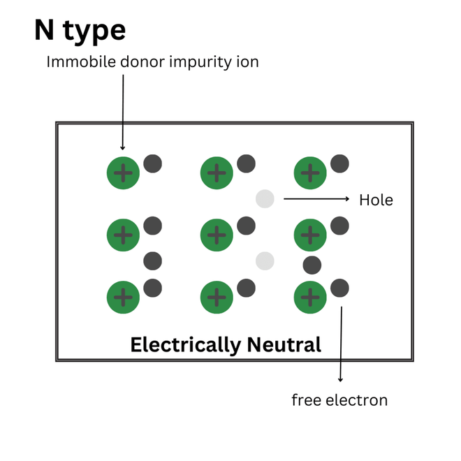
N-type Semiconductors
In N-type Semiconductors, the semiconductor material is doped with atoms from Group V of the periodic table, such as phosphorus (P) or arsenic (As). These dopant atoms have one extra valence electron compared to the semiconductor material. When they replace some of the semiconductor atoms, they create extra electrons in the crystal lattice.
- Conductivity is mainly because of electrons.
- The material is entirely neutral.
- The current (I) is due to electron current (Ie), and the concentration of electrons (ne) is much greater than that of holes (nh).
- Majority carriers are electrons, and minority carriers are holes.
P-type Semiconductors
In order to form p type Semiconductor, trivalent impurity is added to it. These elements have three electrons in there valence shell and need 1 more electron. These are from Group III of the periodic table, such as Boron (B) or Aluminum (Al). These dopant atoms have one less valence electron compared to the semiconductor material. When they are added in semiconductor atoms they take one electron and create holes in the crystal lattice.
- Conductivity is mainly because of the holes.
- The material is entirely neutral.
- The current (I) is due to hole current (Ih), and the concentration of holes (nh) is much greater than that of electrons (ne).
- Majority carriers are holes, and minority carriers are electrons.
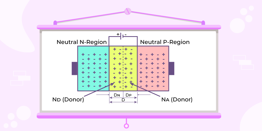
Formation of PN Junction by N and P type Semiconductor

PN Junction Forward Bias
- Creating P and N type Semiconductor by doping: P type semiconductor can be formed by doping the pure semiconductor such as germanium or silicon by adding impurities In P type Group 3 elements are added such as boron Aluminium. N type semiconductor can be made by adding impurities from atoms of Group 5 such as arsenic or phosphorus.
- Bringing the created N and P type Semiconductor together: We need to take the p and n type semiconductor closer in order to form PN Junction. The free electrons of negative N type region will move towards the P type semiconductor and the holes move in opposite direction towards n type region. The holes and the electrons recombine with each other a form a region where no free mobile charge carriers(charge carriers which have movement ) are present it is known as depletion region.
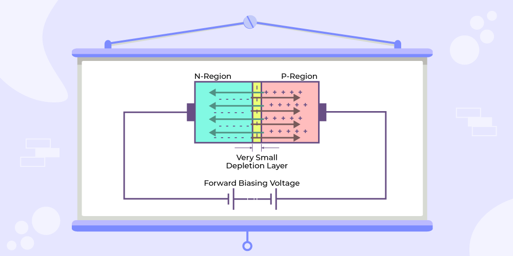
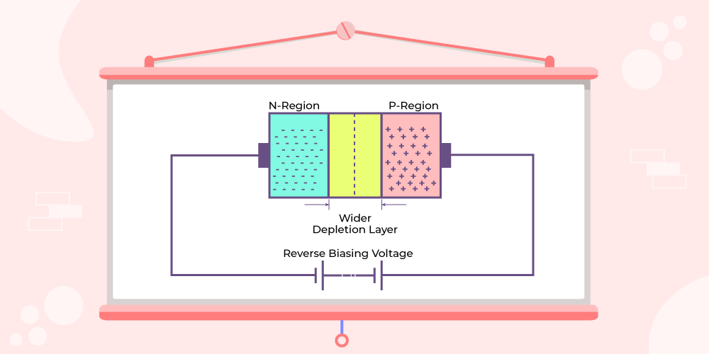
In a forward bias, when a positive voltage is applied to the P-side and negative voltage to the N-side, the potential barrier is reduced, and current can flow across the junction. In reverse bias, where the P-side is negative and the N-side is positive, the potential barrier increases, and the junction prevents significant current flow.
Difference Between Intrinsic and Extrinsic Semiconductor
Here are the main differences between Intrinsic and Extrinsic Semiconductor:
Intrinsic Semiconductor | Extrinsic Semiconductor |
|---|---|
intrinsic semiconductor is a pure semiconductor material like silicon or germanium. | An extrinsic semiconductor has added impurities (dopants) to change its electrical properties. |
In intrinsic semiconductors, thermal energy moves electrons to the conduction band, creating electron-hole pairs. | Extrinsic semiconductors can be N-type (more electrons) or P-type (more holes), based on the additives used. |
At typical temperatures, intrinsic semiconductors exhibit low conductivity due to the constrained count of charge carriers generated by thermal effects. | Extrinsic semiconductors have much higher conductivity than intrinsic ones because doping adds more charge carriers. |
Intrinsic semiconductors have a relatively large energy gap between their valence and conduction bands compared to extrinsic semiconductors. | Doping can also marginally alter the energy gap of extrinsic semiconductors, particularly in the presence of specific additives. |
Intrinsic semiconductors aren’t very conductive, so they’re not used much in devices. But they’re important for understanding how semiconductors work. | Extrinsic semiconductors are used in many electronics like transistors and solar cells because they have controllable high conductivity. |
For More: Difference Between Intrinsic and Extrinsic Semiconductor
Applications of Semiconductor
Semiconductor materials are very useful in our everyday live below are some common examples-
- Computers: The chips and microprocessors which are called the core of computer are made of of semiconductors. These are the parts which helps the computers in processing data. Complex operations are not possible without these chips.
- Use in electronic devices: Basic electronic devices which we use such as Switches, electric circuits, diodes, transistors are made using semiconductors
- Light-emitting diodes (LEDs): LEDs are used in home for lightning these are semiconductor devices which produce light when current is passed through them. LEDs are used in everyday lighting applications, including energy-efficient bulbs for homes and offices, as well as in traffic signals, vehicle headlights, and electronic displays.
- Wearable Technology: The wearable devices such as smart watches now in latest smart rings have been built they are only possible using semiconductor technology. Because in them microprocessor chips are used which can be made using semiconductors
- Home Automation: Semiconductors are a crucial part of home automation systems, allowing for smart home devices like smart thermostats, smart lighting, smart security cameras, and voice-activated virtual assistants.
Uses of Semiconductors in Everyday Life
Given below are the day to day uses of Semiconductors
- Computers and Laptops: The CPUs and GPUs are made from Semiconductor technology.
- Televisions: The Modern day LED and OLED are made from Semiconductor materials.
- Communication: Many communication devices such as Routers ,Modems, Satellite and GPS Systems are made from semiconductor chips.
- Lighting: Lighting systems such as LED Light are made from semiconductor materials.
Importance of Semiconductors
Importance of Semiconductors are
- Small Size: The Semiconductors are manufactured at microscopic scales which can be used for creating compact and portable device.
- Low Power Consumption: The Semiconductors require less input power compared to other technologies.
- Shockproof: Semiconductor devices are solid-state and have no moving parts which make them resistant to physical shocks and vibrations.
- Long Lifespan: The Semiconductors have large lifespan as compared to other technologies.
- Noise-Free Operation: The Semiconductor devices works with less electrical noise which improves its performance.
Advantages of Semiconductor
Here are some advantages of a semiconductor:
- Miniaturization: Semiconductors are used in extremely small devices such as microprocessors and chips. They allows miniaturization in so that the devices which took a lot of space, with help of semiconductors can be made in small sizes.
- Energy Efficiency: As compared to other materials semiconductor is an energy efficient device. They consume lower energy compared to other materials while the electronic operations are performed.
- Light Emission: Certain semiconductor have the property to emit light when the electric current is passed through them. This made the LEDs (Light Emitting Diodes) possible and also the laser diodes.
- High Switching Speed: The switching speed in semiconductors in comparatively very high which allows fast switching in devices. This is important property because it saves time and lowers the complexity and also allows them to perform fast digital operations.
- Formation of IC: Integrated circuits (ICs) can incorporate millions of semiconductor devices on a single chip, leading to complex functionalities in a compact form.
Disadvantages of Semiconductor
Some of the disadvantages of a Semiconductor are:
- Temperature Vulnerability: Semiconductor gadgets can react strongly to changes in temperature, leading to shifts in how they work and how dependable they are.
- Expensive Production: Making semiconductors involves intricate processes and specialized facilities, resulting in high initial manufacturing expenses.
- Heat Tolerance Limits: Some semiconductors can’t endure high temperatures well. This could lead to their performance dropping or even failing.
- Reliance on Purity: The efficiency of semiconductors heavily depends on how pure they are. Even minor impurities can drastically change their electrical characteristics.
- Issues with Consistency: Over time, specific semiconductor devices might degrade or wear out, negatively affecting their dependability and lifespan.
Solved Examples of Semiconductor
Calculate the electron concentration in a silicon semiconductor at room temperature (300 K) assuming the conduction band edge energy (Ec) is:- 1.12 eV and the Fermi energy (Ef) is 0.5 eV.
n = Nc * exp((1.12 eV – 0.5 eV) / (8.6173 × 10^-5 eV/K * 300 K))
(Values of Nc and constants should be looked up in a semiconductor physics reference for accurate calculations.)
d)Drift Current Density (Jd) Formula:
Jd = q * n * μ * E
Where Jd = Drift current density
- q = Elementary charge
- n = Carrier concentration
- μ = Mobility of carriers
- E = Electric field
Calculate the drift current density in a semiconductor with carrier concentration n = 1.5 x 10^16 cm^-3, mobility μ = 1000 cm^2/Vs, and electric field E = 200 V/cm.
Jd = (1.6 x 10^-19 C) * (1.5 x 10^16 cm^-3) * (1000 cm^2/Vs) * (200 V/cm)
= 4.8 x 10^-2 A/cm².
Conclusion
he chemical and electrical properties of Semiconductors help them to serve for the electronic devices LEDs , solar cell, etc. Without the use of the semiconductors, life would be complex and different. Semiconductor material the main reason behind them is they have moderate and controlled conductivity which can be changed by doping. Semiconductors have unique properties which make it favorable for making a lot of devices from them.
Semiconductor – FAQs
Who invented semiconductor?
Karl Braun in 1874.
What is the effect of heating on resistance of Semiconductor?
The resistance will decrease.
Highlight some advantages of Semiconductor devices?
Semiconductor devices are small in size, its low power consumption, higher reliability, fast switching speed, and ease of integration, making them the foundation of modern electronics and technology.
What recent advancements have impacted Semiconductor technology?
Some recent developments include the use of wide-bandgap semiconductors (like SiC and GaN) for power electronics and the exploration of novel materials, such as perovskite, for high-efficiency solar cells. Hence semiconductors are continuously evolving over time in form of there fabrication methods, device design etc.
What are the 2 most used semiconductors?
The two most commonly used semiconductors are:
- Silicon (Si)
- Gallium arsenide (GaAs)
What is the resistivity of pure silicon?
6000 Ω cm
How much impurity is added in extrinsic semiconductor as compared to intrinsic pure semiconductor?
1 atom for 108 atoms
What is Intrinsic Semiconductor ?
Intrinsic semiconductors are semiconductors that are pure i.e. it does not contain any impurity. Since it does not contain any impurity, the number of free electrons and the number of holes are equal. It is also known as an i-type semiconductor. The number of free electrons and the number of holes depends on the property of the material and does not depend on the doping.
For intrinsic semiconductors
n = pwhere, n=number of electron, m=number of holes.
On the basis of electrical conductivity, materials are classified as:
- Conductors: Good conductors of electricity
- Insulators: Bad conductors of electricity
- Semiconductors: These materials have conductivity levels between those of conductors and insulators.
On the basis of the amount of doping, semiconductors are Classified as:
- Intrinsic Semiconductors
- Extrinsic Semiconductors
Example of Intrinsic Semiconductors :
Silicon and germanium are the best examples of Intrinsic semiconductors.
Free Electrons and Holes
Electrons that are available, for the flow of the current, above 0 Kelvin or above -273 degree Celcius is known as free electrons. Above 0 kelvin, these electrons gain energy and cross the energy band gap, leaving behind an empty space. This empty space is known as a hole. Holes are treated as +ve charges because there is a deficiency of -ve charge at that place.
How do Intrinsic Semiconductors Work?
To understand the working mechanism of intrinsic semiconductors, we need to know the electronic configuration of their atoms.
The electronic configuration of silicon and germanium are:
1. Silicon –> 1s2 2s2 2p6 3s2 3p2
2. Germanium –> 1s2 2s2 2p6 3s2 3p6 4s2 3d10 4p2
We can clearly see that the outermost shell is having 4 electrons. At 0 Kelvin, the semiconductor behaves like a pure insulator. Now, with the increase in the temperature, electrons gain enough energy to free from its shell and leave behind an empty place known as a hole. Thus, a free electron is produced along with a hole.This is the reason for the equal number of electrons and holes in intrinsic semiconductors.
Key Points of Intrinsic Semiconductors
- Intrinsic semiconductors uses electrons and holes for conduction at room temperature.
- At 0 Kelvin (absolute temperature), intrinsic semiconductors behave like pure insulators.
- When an intrinsic semiconductor is doped with an impurity, it gets converted into an extrinsic semiconductor.
Extrinsic Semiconductor
As we all know, based on conductivity, we divide the material into three categories: Conductor, Semiconductor, and Insulator. In which the conductivity of the conductor is highest, insulators have the lowest conductivity, and semiconductors have intermediate conductivity. The reason behind this is the number of free electrons present in the crystal of each material. If we talk about the conductivity of semiconductors, two different types of semiconductors are classified based on the number of electrons and holes present in the crystal: Intrinsic and Extrinsic semiconductors. In this article, we will discuss these semiconductors, especially extrinsic semiconductors, their properties, formation, needs, and various applications.
What are Semiconductors?
It is defined as the material that shows both the properties of the conductor and the insulator in different conditions. The conductivity of a semiconductor lies between the conductor and the insulator. Some examples of elementary semiconductors are silicon (Si) and germanium (Ge).
Energy Band Theory
Based on Pauli’s exclusion principle, the energy of an electron is definite in a single isolated atom, but after the formation of a molecule or crystal, the energy of an electron is not fixed but varies in some range, which is called the energy band. There are two important bands: The valence band and the Conduction band, respectively.
- Valence band: It represents the energy of bonded electrons, which are present in the valence band and do not take part in conduction.
- Conduction band: It represents the energy of free electrons, which are present in the conduction band and take part in conduction.
- Forbidden energy gap: It is defined as the energy gap between the valence and conduction band, and it is known as forbidden because no electron is present inside this energy gap. It is represented as ΔEg.
Classification of solids based on energy band theory:
-(2)-(1)-660.png)
Classification of solids based on energy band theory
Effect of Temperature on Semiconductor
- Case 1: When the temperature is equal to 0k.
At T = 0k, all the valence electrons are bound in the valence band, and no electron is free to move in the crystal, as a result of which the semiconductor behaves as a perfect insulator.
- Case 2: When the temperature is greater than 0k.
At T > 0k, due to thermal energy some covalent bonds break and electrons are free to move in the crystal, leaving behind a vacancy called a hole. Due to the generation of electron-hole pair in the crystal, the semiconductor behaves as a conductor.
Properties of Semiconductors
- There are two charge carriers present in the semiconductors, i.e. an electron and a hole.
- The hole is considered the imaginary charge carrier in the semiconductor.
- Electrons and holes both have the same magnitude of charge but opposite signs.
- The mobility of a hole is less than the mobility of an electron.
- The net current of the semiconductor is due to the movement of electrons and holes, i.e Itotal = Ie + Ih
- The net conductivity of a semiconductor is also due to both charge carriers, i.e σtotal = σe + σh
Types of Semiconductors
Based on the number of electrons and holes, there are two types of semiconductors: Instrinc and Extrinsic
Intrinsic semiconductor
A semiconductor in which the number of electrons is equal to the number of holes is known as an intrinsic semiconductor. It is also known as a pure semiconductor because there exists no impurity that has been added to this semiconductor.
Condition for intrinsic / Pure semiconductor: ne = nh = ni
where ne = number of electrons
nh = number of holes
ni = intrinsic carrier concentration
As the number of electrons and holes are equal in the intrinsic semiconductor, it is electrically neutral.
At room temperature, the conductivity of intrinsic semiconductors is very low, and it is not fit for designing any practical devices.
What is Doping?
As we discussed, the conductivity of intrinsic semiconductors is very low, so to increase the conductivity of the semiconductor we add some impurity atoms to the semiconductor, which are known as dopants, and the process is known as doping.
Conditions for doping:
- The doping ratio must be equal to 1 ppm (1 part per million), that means for every 106 pure atoms there exists 1 impure atom, i.e. 106: 1
- The size of a dopant / impure atom must be equal to the size of a pure atom, to maintain the crystal structure.
b) Extrinsic Semiconductor
A semiconductor in which the number of electrons and holes are unequal is known as an extrinsic semiconductor. An extrinsic semiconductor is formed by adding the impure atom or dopant to the pure semiconductor. It is also known as an impure and doped semiconductor.
Extrinsic / Impure / Doped semiconductor = Instrinsic / Pure semiconductor + Dopants
In extrinsic semiconductors, doping is done to increase the conductivity of semiconductors, so we can use them to create some practical devices. If we consider Silicon or Germanium as our semiconductor, there are two different groups of elements that are suitable for use as dopants, Group 13 (BORON FAMILY) & Group 15 ( NITROGEN FAMILY) based on the conditions of doping.
Types of Extrinsic Semiconductor:
Depending on the type of dopants we use, there are two different types of extrinsic semiconductors formed:
- N-type extrinsic semiconductor
- P-type extrinsic semiconductor
N-type semiconductor
It is formed when pentavalent impurities were added to the semiconductor. It is also known as donor impurity.
When any dopant atom is added to a semiconductor crystal, like silicon, it replaces the silicon atom and makes a bond with another silicon atom, when we add a pentavalent impurity, five out of four electrons are only able to make the bond with their neighboring silicon atom, but that one extra electron is not able to make any bond, and it freely moves in the entire semiconductor crystal. As a result of which, the conductivity of semiconductors increases. As we see by adding a pentavalent impurity to the semiconductor, it donates an electron in the crystal, and that is why it is also known as a donor impurity atom.
Examples of pentavalent dopant atoms are Phosphorus, Arsenic Antimony, etc.
In N type semiconductor, the majority charge carriers are electrons and minority charge carriers are holes.
Condition in N type semiconductor : Ne >>> Nh
Therefore the current in N type semiconductor is due to electrons only, Itotal ≅ Ie.
And the conductivity is also due to electrons only σtotal ≅ σe
Ne ≅ ND where ND is Donar atom density
The block diagram of an N-type semiconductor:
Block diagram of an N-type Semiconductor
The energy level diagram of an N-type semiconductor:
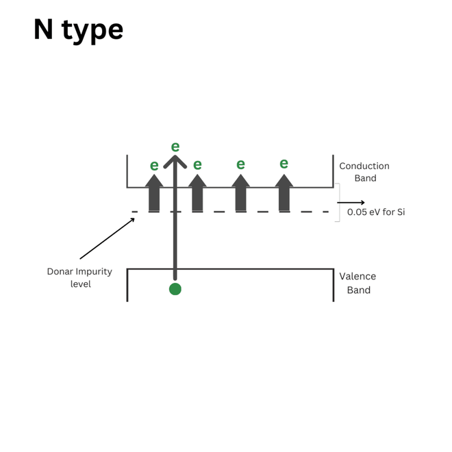
The energy level diagram of an N-type semiconductor
b) P-type semiconductor
It is formed when trivalent impurities(Boron family) were added to the semiconductor. It is also known as acceptor impurity. When any dopant atom is added to a semiconductor crystal, like silicon, it replaces the silicon atom and makes a bond with another silicon atom, and when we add a trivalent impurity, all three electrons make bonds with the neighboring silicon atom and a vacancy is created in the semiconductor crystal known as a hole. All the neighboring electrons try to fill this vacancy, resulting in a creation of a new vacancy at their site. This is how the movement of the hole takes place. As a result of which, the conductivity of semiconductors increases. As we see by adding a trivalent impurity to the semiconductor, it accepts an electron from the crystal, and that is why it is also known as an acceptor impurity atom.
Examples of trivalent dopant atoms are Boron, Aluminium, Indium, etc.
In P type semiconductor, the majority charge carriers are holes and minority charge carriers are electrons.
Condition in P type semiconductor : Nh >>> Ne
Therefore the current in P type semiconductor is due to holes only, Itotal ≅ Ih.
And the conductivity is also due to holes only σtotal ≅ σh
Nh ≅ NA where NA is Acceptor atom density
The block diagram of a P-type semiconductor:

Block diagram of a P-type semiconductor
The energy level diagram of a P-type semiconductor:
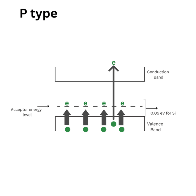
The energy level diagram of a P-type semiconductor
Conclusion
In this article, we learn that a semiconductor is a type of material that shows both the property of conductors and insulators, its classification is based on energy band theory and different properties like having two different charge carriers: electron and hole respectively. Then we classify semiconductors into two different types: intrinsic and extrinsic, based on the number of electrons and holes present in the crystal. Due to the low conductivity of intrinsic semiconductors, we made extrinsic semiconductors by adding some impure atoms in them, to increase their conductivity, and this leads to the formation of two different types of extrinsic semiconductors: N and P-type semiconductors. In N-type semiconductors, the majority charge carriers are: electrons and minority charge carriers are: holes. On the other hand in P-type semiconductors, the majority of charge carriers are: holes and the minority of charge carriers are: electrons. Extrinsic semiconductors are used in various practical devices such as P-N Diode, ICs, Solar cells, sensors, and in detectors.
FAQs on What is Extrinsic Semiconductor?
Q.1: Does extrinsic semiconductors are electrically neutral?
Answer:
Yes, extrinsic semiconductors are electrically neutral, although the number of electrons and holes are unequal the electrical neutrality is maintained in both the N and P type of semiconductor.
Q.2: What is Mass-Action law?
Answer:
It defines the relationship between ne, nh, and ni . According to mass action law, At thermal equilibrium, the product of the concentration of electrons and holes is equal to the square of intrinsic concentration.
Q.3: Do holes moves in a crystal?
Answer:
In actual, electrons are moving in order to fill the vacancy (holes) in the crystal, leaving behind a vacant at their lattice site, but it appears that holes are moving, which is not the real case.
Q.4: List some applications of extrinsic semiconductors.
Answer:
Due to high conductivity and application in making of practical devices, extrinsic semiconductor are used in various applications like:
- P-N Diodes
- Integrated Circuits
- LEDs
- Electronic Detectros
- Sensor
PN Junction Diode
The electrical conductivity of a semiconductor material is between that of a conductor, such as metallic copper, and that of an insulator, such as glass. Its resistivity decreases as the temperature rises, whereas metals have the reverse effect. By adding impurities (doping) into the crystal structure, its conducting characteristics can be changed in beneficial ways. Diodes, transistors, and most contemporary electronics are built on the behaviour of charge carriers such as electrons, ions, and electron holes at these junctions.
Silicon, germanium, gallium arsenide, and elements along the periodic table’s so-called metalloid staircase are examples of semiconductors. Gallium arsenide is the second most common semiconductor after silicon, and it is used in laser diodes, solar cells, microwave-frequency integrated circuits, and other applications. Silicon is a crucial component in the production of most electrical circuits.
P-N Junction
Inside a semiconductor, a p-n junction is an interface or a border between two semiconductor material types, namely the p-type and the n-type.
The semiconductor’s p-side, or positive side, has an excess of holes, whereas the n-side, or negative side, has an excess of electrons. The doping process is used to produce the p-n junction in a semiconductor.
Formation of P-N Junction
When we utilize various semiconductor materials to form a p-n junction, there will be a grain boundary that will prevent electrons from moving from one side to the other by scattering electrons and holes, which is why we employ the doping procedure.
For example, Consider a p-type silicon semiconductor sheet that is very thin. A portion of the p-type Si will be changed to n-type silicon if a tiny quantity of pentavalent impurity is added. This sheet will now have both a p-type and an n-type area, as well as a junction between the two. Diffusion and drift are the two sorts of processes that occur following the creation of a p-n junction. As we all know, the concentration of holes and electrons on the two sides of a junction differs, with holes from the p-side diffusing to the n-side and electrons from the n-side diffusing to the p-side. This causes a diffusion current to flow across the connection.
When an electron diffuses from the n-side to the p-side, it leaves an ionized donor on the n-side, which is stationary. On the n-side of the junction, a layer of positive charge develops as the process progresses. When a hole is moved from the p-side to the n-side, an ionized acceptor is left behind on the p-side, causing a layer of negative charges to develop on the p-side of the junction. The depletion area is defined as a region of positive and negative charge on each side of the junction. An electric field direction from a positive charge to a negative charge is generated due to this positive space charge area on each side of the junction. An electron on the p-side of the junction travels to the n-side of the junction due to the electric field. The drift is the name given to this motion. We can observe that the drift current runs in the opposite direction as the diffusion current.
Biasing Conditions for p-n Junction Diode
In a p-n junction diode, there are two operational regions:
- p-type
- n-type
The voltage applied determines one of three biasing conditions for p-n junction diodes:
- There is no external voltage provided to the p-n junction diode while it is at zero bias.
- Forward bias: The p-type is linked to the positive terminal of the voltage potential, while the n-type is connected to the negative terminal.
- Reverse bias: The p-type is linked to the negative terminal of the voltage potential, while the n-type is connected to the positive terminal.
Forward Biased PN Junction
The p-n junction is said to be forward-biased when the p-type is connected to the positive terminal of the battery and the n-type to the negative terminal. The built-in electric field at the p-n junction and the applied electric field are in opposing directions when the p-n junction is forward biased.
The resulting electric field is smaller than the built-in electric field when both electric fields are added together. As a result, the depletion area becomes less resistant and thinner. When the applied voltage is high, the resistance of the depletion zone becomes insignificant. At 0.6 V, the resistance of the depletion area in silicon becomes absolutely insignificant, allowing current to flow freely over it.
Reverse Biased PN Junction
The p-n junction is said to be reverse-biased when the p-type is linked to the negative terminal of the battery and the n-type is attached to the positive side. The applied electric field and the built-in electric field are both in the same direction in this situation.
The resultant electric field is in the same direction as the built-in electric field, resulting in a more resistive, thicker depletion zone. If the applied voltage is increased, the depletion area gets more resistant and thicker.
P-N Junction Formula
The p-n junction formula, which is based on the built-in potential difference generated by the electric field, is as follows:
where,
- The zero-bias junction voltage is E0.
- At room temperature, VT is the thermal voltage of 26 mV.
- The impurity concentrations are denoted by the letters ND and NA.
- The intrinsic concentration is denoted by ni
Current Flow in PN Junction diode
When the voltage is increased, electrons move from the n-side to the p-side of the junction. The migration of holes from the p-side to the n-side of the junction occurs in a similar manner as the voltage rises. As a result, a concentration gradient exists between the terminals on both sides.
There will be a movement of charge carriers from higher concentration regions to lower concentration regions as a result of the development of the concentration gradient. The current flow in the circuit is caused by the movement of charge carriers inside the p-n junction.
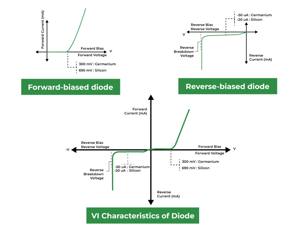
VI Characteristics of PN Junction Diode
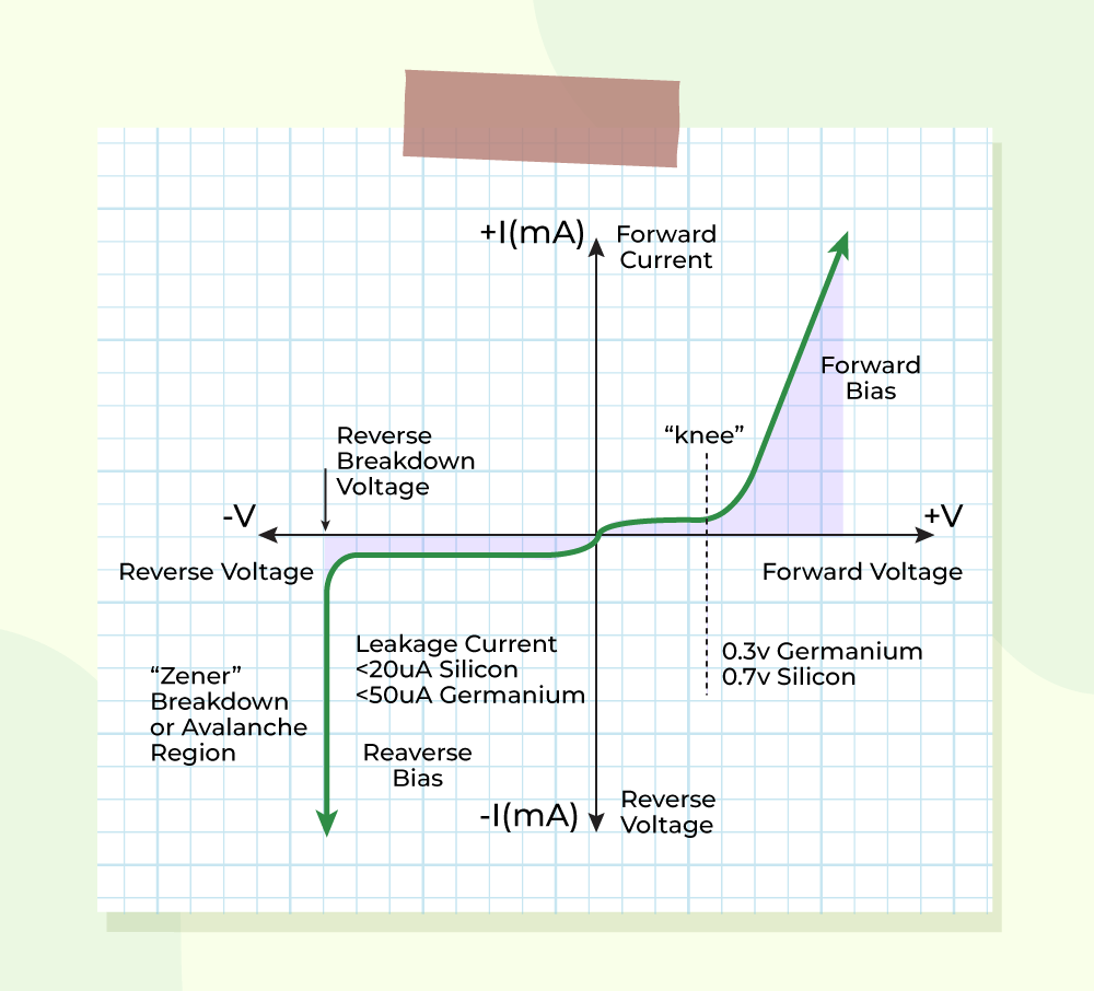
A curve between the voltage and current across the circuit defines the V-I properties of p-n junction diodes. The x-axis represents voltage, while the y-axis represents current. The V-I characteristics curve of the p-n junction diode is shown in the graph above. With the help of the curve, we can see that the diode works in three different areas, which are:
- Zero bias
- Forward bias
- Reverse bias
Zero Bias
There is no external voltage provided to the p-n junction diode while it is at zero bias, which implies the potential barrier at the junction prevents current passage.
Forward bias
When the p-n junction diode is in forwarding bias, the p-type is linked to the positive terminal of the external voltage, while the n-type is connected to the negative terminal. The potential barrier is reduced when the diode is placed in this fashion. When the voltage is 0.7 V for silicon diodes and 0.3 V for germanium diodes, the potential barriers fall, and current flows.
The current grows slowly while the diode is under forwarding bias, and the curve formed is non-linear as the voltage supplied to the diode overcomes the potential barrier. Once the diode has crossed the potential barrier, it functions normally, and the curve rises quickly as the external voltage rises, yielding a linear curve.
Reverse Bias
When the PN junction diode is under negative bias, the p-type is linked to the negative terminal of the external voltage, while the n-type is connected to the positive terminal. As a result, the potential barrier becomes higher. Because minority carriers are present at the junction, a reverse saturation current occurs at first.
When the applied voltage is raised, the kinetic energy of the minority charges increases, affecting the majority charges. This is the point at which the diode fails. The diode may be destroyed as a result of this.
Applications of PN Junction Diode
There are various applications of PN Junction Diode in the field of electronics, some of those applications are listed as follows:
- A most common use case of a PN junction diode is as a rectifier which means converting AC current into DC current.
- Zener diode (which is a special type of PN junction diode) is used in circuits for voltage regulation.
- As Diode only conducts current in Forward bias, so in electrical circuits, it is used as a switch to turn on and off certain small circuits in a much more complex circuit.
- A reverse-biased p-n junction diode is utilized as a photodiode as it is sensitive to light.
- LED is also a special type of PN junction diode on a forward basis which emits light.
Sample Questions on PN Junction Diode
Question 1: What is reverse resistance?
Answer:
The resistance supplied by a p-n junction diode when it is reverse biased is known as reverse resistance.
Question 2: What is a diode’s dynamic resistance?
Answer:
The ratio of change in voltage to change in current is known as dynamic resistance of a diode.
Question 3: What is a diode’s static resistance?
Answer:
The ratio of the DC voltage put across the diode to the DC current flowing through it is known as the diode’s static resistance.
Question 4: What is reverse bias?
Answer:
When the p-type is connected to the negative terminal of the battery and the n-type is connected to the positive side, the p-n junction is said to be reverse biased. In this case, the applied electric field and the built-in electric field are both pointing in the same direction. Because the generated electric field is in the same direction as the built-in electric field, the depletion zone becomes more resistive and thicker. The depletion region becomes more resistive and thicker as the applied voltage is raised.
Question 5: What is forward bias?
Answer:
When the p-type is linked to the positive terminal of the battery and the n-type to the negative terminal, the p-n junction is said to be forward-biased. When the p-n junction is forward biased, the built-in electric field and the applied electric field are in opposite directions. When both electric fields are put together, the resulting electric field is smaller than the built-in electric field. As a result, the depletion zone grows narrower and less resistive. The resistance of the depletion zone becomes negligible when the applied voltage is large. At 0.6 V, the resistance of the depletion region in silicon is negligible, enabling current to readily flow through it.
FAQs on PN Junction Diode
Q1: What is PN Junction?
Answer:
A PN junction is a junction formed by joining a p-type semiconductor and an n-type semiconductor. It is the basic building block of many electronic devices, including diodes, transistors, solar cells, and LEDs.
Q2: What is the depletion region in the p-n junction?
Answer:
The depletion region is a region that forms at the interface of a p-type and n-type semiconductor in a PN junction when they are joined together. It is a region that has a very low concentration of charge carriers and is depleted of mobile charge carriers.
Q3: What is PN Junction Diode?
Answer:
A PN junction diode is a two-terminal electronic device that is made up of a PN junction. It is the simplest form of semiconductor device and is used as a rectifier, voltage regulator, and switch in various electronic circuits.
Q4: When a p-n junction is reverse biased?
Answer:
A p-n junction is reverse biased when the voltage applied across it is such that the positive terminal of the battery is connected to the n-type semiconductor and the negative terminal is connected to the p-type semiconductor. In this condition, the depletion region becomes wider and the flow of electric current is reduced.
Q5: When p-n junction is kept in forward bias?
Answer:
A p-n junction is reverse biased when the voltage applied across it is such that the positive terminal of the battery is connected to the n-type semiconductor and the negative terminal is connected to the p-type semiconductor. In this condition, the depletion region becomes wider and the flow of electric current is reduced.
Q6: What happens in a P-N junction diode in a Reverse-Biased condition?
Answer:
In the reverse-biased condition in a P-N junction diode, the holes and electrons tend to move away from the junction.
Diode
A diode is an electronic device that conducts electricity only in one direction. It is a device which is widely used in modern-day electronics. In this article, we will learn about diodes, their properties, symbols, types and others in detail.
What is a Diode?
A diode is made up of two words i.e., “Di “ means Two, and “Ode “ means Electrodes which means that a device or component has two electrodes. (i.e., cathode and anode). A diode is an electronic device having a two-terminal unidirectional power supply i.e it has two terminals and allows the current to flow only in one direction. Diodes are widely used in modern-day circuits to secure circuits from over-voltage and they are also used to change AC current to DC current.
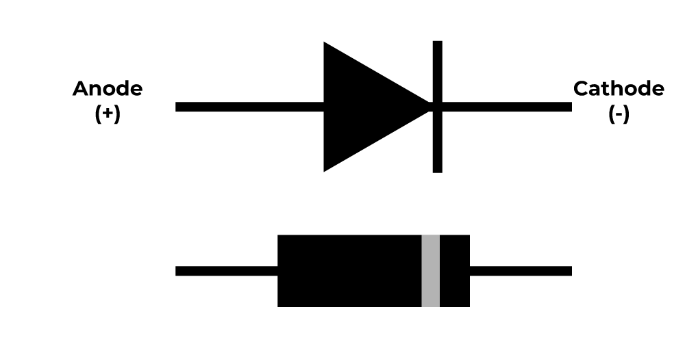
Representation Symbol of a Diode
Diodes are represented using special symbols and the symbol for a standard diode symbol is given below. In the given diagram it is clear that a diode has two terminals which are called the cathode and anode. The arrowhead symbol represents the anode and the other end represents the cathode. The current flow from anode to cathode in the forward bias condition. The general representation of a Diode is given below,
Construction of Diode
We know that there are two types of semiconductor materials: Intrinsic and Extrinsic semiconductors. In intrinsic semiconductors, the number of electrons and hole concentration are equal at room temperature. In an extrinsic semiconductor, impurities are added to the semiconductor to increase the number of electrons or the number of holes. These impurities are pentavalent (Arsenic, Antimony, phosphorous) or tri-valent (boron, indium, aluminium).
A semiconductor diode has two layers. one layer is of p-type and the other is of n-type semiconductor.
- If we add trivalent impurities in a semiconductor (Silicon and germanium), a greater number of holes are present and it is a positive charge. therefore this type of layer is known as the p-type layer.
- If we add pentavalent impurities in semiconductors (silicon or germanium), due to excess electrons there is a negative charge. therefore this type of layer is known as the n-type layer.
Working of Diode
In the N-type region, the majority of charge carriers are electrons and the minority of charge carriers are holes. Whereas, In the P-type region, the majority of charge carriers are holes and the minority of charge carriers are electrons. Because of the concentration difference, the diffusion takes place in majority charge carriers and they recombine with the minority charge carriers which are then collected near the junction and this region is known as the Depletion Region.
- When the anode or p-type terminal of the diode is connected with a negative terminal and the n-type or cathode is connected with the positive terminal of a battery, this type of connection is called a Reverse Bias condition.
- When the anode or p-type terminal of the diode is connected with a positive terminal and the n-type or cathode is connected with the negative terminal of the battery, this type of connection is called a Forward Bias condition.
Characteristics of Diode
The characteristics of the diode can easily be understood under the following three headings.
- Forward-Biased Diode
- Reverse-Biased Diode
- Zero Biased Diode OR Unbaised Diode
Forward-Biased Diode
In forward biasing semiconductor is connected to an external source when the p-type semiconductor is connected to the positive terminal of the source or battery and the negative terminal to the n-type, then this type of junction is said to be forward-biased. In forward bias, the direction of the built-in electric field near the junction and the applied electric field are opposite in direction. This means that the resultant electric field has a magnitude lesser than the built-in electric field due to this there is less resistivity and therefore depletion region is thinner. In silicon, at the voltage of 0.6 V, the resistance of the depletion region becomes completely negligible.
Reverse-Biased Diode
In reverse biasing, the n-type is connected to the positive terminal and the p-type is connected to the negative terminal of the battery. In this case, the applied electric field and the built-in electric field are in the same direction and the resultant electric field has a higher magnitude than the built-in electric field creating a more resistive, therefore depletion region is thicker. if the applied voltage becomes larger, then the depletion region becomes more resistive and thicker.
The V-I characteristic of a diode in forward and reverse-biased conditions are,
Zero Biased Diode OR Unbaised Diode
When there is no external source applied to semiconductors is known as an unbiased diode. the electric field is built up across the depletion layer between the p-type and the n-type material. this happens because of the unbalanced no. of electrons and holes due to doping. At room temperature, for a silicon diode, 0.7V is the barrier potential.
Ideal Diodes
Ideal diodes are diodes that are used to control the direction of current flow. An ideal diode allows current to flow in one direction only, called the forward direction whereas the current flowing in the reverse direction is blocked.
In the reverse biased condition, the ideal diodes look like an open circuit and in this condition the voltage across the diode is negative.
Types of Semiconductor Diode
There are different types of semiconductor diodes that are used widely in our daily life some of which are,
- LED
- P-N Junction Diode
- Zener Diode
- Photodiode
- Schottky Diode
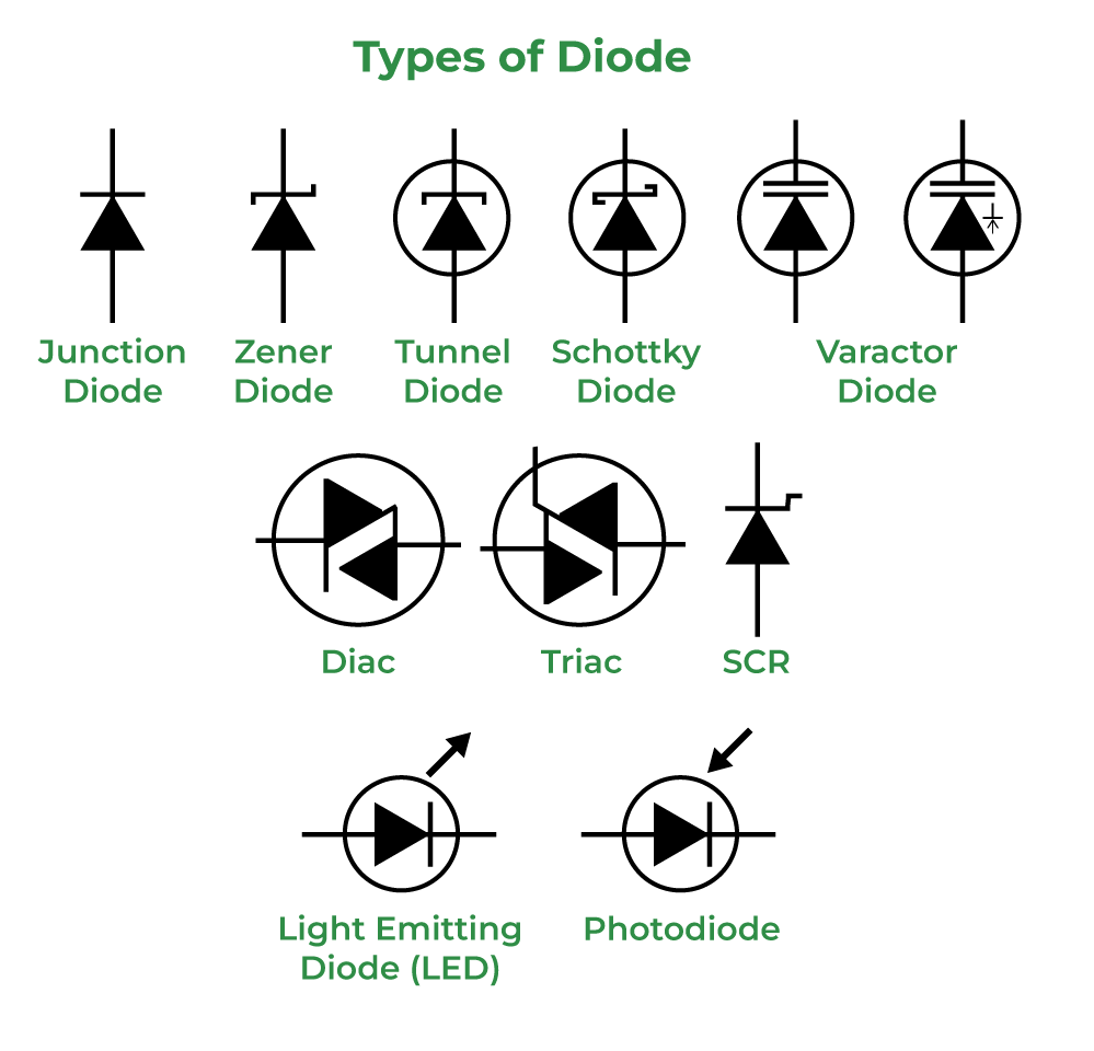
LED
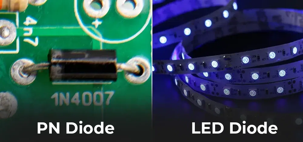
LED is also called a Light Emitting Diode, it is the most useful kind of diode when the diode is attached in forwarding bias, the then-current that flows through the junction produces light and hence they are widely used as bulbs for providing light.
P-N Junction Diode
P-N junction diodes also called rectifier diodes are used for the rectification process. In a P-N junction diode, two layers of semiconductors materials are used. For a P-N junction diode, one layer is made of P-type semiconductor material and the other layer of N-type material. The combination of these two layers forms a junction known as the P-N junction. Thus, the name comes P-N junction diode.
The current in the P-N junction diode flows in the forward-biased condition and blocks in the reverse-biased condition.
Learn more on, VI Characteristics of a P-N Junction Diode
Zener Diode
Zener diode is a type of diode, that allows the flow of current in a forward direction, and it can also work in reverse conditions, the Zener diode has an application in voltage regulation, The Zener diode is a heavily doped p-n junction diode made to work in reverse bias condition.
Schottky Diode
Schottky Diodes are special P-N junction diodes that are made to work in low-voltage regions ideally in voltage ranges between 0.15 and 0.4 volts. These are made differently to obtain maximum performance at low voltage. Schottky diodes are highly used in rectifier applications.
Variable Capacitance Diode
This kind of diode is also called a VARICAP diode, even though the output of variable capacitance can exhibit the general p-n junction diode but this diode is approved of giving the preferred capacitance change as they are different types of the diode.
Photodiode
The photodiode produces current when a certain amount of light energy falls over them, They are special diodes that can detect any light that falls on them. They work in reverse bias conditions and are used in solar cells and photometers.
Applications of Semiconductor Diode
Semiconductor Diode have all sorts of applications and some of the applications of semiconductor diodes are as follows:
- Rectifier Diode: A rectifier diode is a kind of diode that is used for the rectification of alternating current (A.C).
- LED: LEDs are diodes used for providing light.
- Zener Diode: Zener diode is used for the stabilization of current and voltage in electronic systems.
- Photodiode: Photodiodes are used to detect light.
- Switching Diode: Switching diodes are used for providing fast switching in circuits.
- Tunnel Diode: A tunnel diode is a special type used in the negative resistance region.
Read, More
FAQs on Diodes
Question 1: What is a diode?
Answer:
A two-terminal electronic device that conducts electricity only in one direction is called a diode.
Question 2: What is doping?
Answer:
Doping is the process of adding impurities into the semiconductor, so that more electron-hole pair are generated. The impurities added, are generally pentavalent and trivalent impurities.
Question 3: Which type of semiconductors are used in manufacturing diodes?
Answer:
Silicon and Germanium semiconductors are most commonly used for the manufacturing of diodes.
Question 4: Which diode is used as a voltage regulator?
Answer:
The Zener diode is generally used as a voltage regulator.
Question 5: Why is Zener Diode used as a voltage regulator?
Answer:
The Zener diode is used as a voltage regulator because it also works in reverse bias conditions.
Question 6: What is the breakdown voltage of the diode?
Answer:
In reverse bias condition, when the applied voltage increases gradually at a certain point there is an increase in reverse current noticed, this is junction breakdown, corresponding applied voltage is known as the breakdown voltage of the p-n junction diode.
Question 7: What are the types of diodes?
Answer:
There are various types of diodes some of the important ones are,
- P-N Junction Diode
- Zener Diode
- Light Emitting Diode (LED)
- Photodiode, etc.
Question 8: What are the applications of diodes?
Answer:
Diodes have various applications some of the important applications and uses of the diode are,
- Diodes are used as a rectifier.
- Diodes are used as a voltage regulators.
- Diodes are used in logical gates.
- Diodes are used in the clipping circuit.
- Diodes are used in clamping circuits.
Rectifier
Rectifier is an electronic component that converts alternating current (AC) into direct current (DC), ensuring a unidirectional flow of electric charge. As we know, electricity reaches our homes from power grids in the form of AC, but most commonly used electric appliances, such as mobile phones, computers, televisions, fridges, etc operate on direct current (DC). Therefore, the rectifier becomes a very useful component in electronics.
This article provides a detailed understanding of the electrical component known as a rectifier, including its types such as full-wave and half-wave rectifiers, controlled and uncontrolled rectifiers, etc. In addition to that, we will learn about various specific rectifiers such as the Mercury Arc Rectifier, Selenium Rectifier, and Precision Rectifiers.
Table of Content
What are Rectifiers?
Rectifiers are electronic devices or circuits that convert alternating current (AC) into direct current (DC). Alternating current periodically changes direction, whereas direct current flows consistently in one direction. Rectifiers are crucial in many electronic applications where a steady DC voltage is required.
Most rectifiers use P-N junction diodes to convert AC to DC, but some use different kinds of materials as well, such as semiconductor materials like silicon carbide or specialized semiconductor devices like thyristors and metal-oxide-semiconductor field-effect transistors (MOSFETs).
How does Rectifier Work?
A rectifier is an electrical device which is used to convert AC current into DC current. Rectifier does this process by allowing current (I) to flow through any device and the process taking place here is called rectification.
Rectifier works by using diodes which are like one-way valves for electricity. A rectifier can take one or more diodes to convert the positive or negative half cycle of the AC inputs DC outputs. Rectifiers generates an DC voltage by rectifying any one cycle of the AC supply and the reverse operation of this above process is called Inverter and the process called inversion in electricity.
Rectifiers Circuits
It plays a vital role in DC power supplies for converting AC signal into DC signal. P-N junction diode have lot of applications and Rectifier circuits are one of them. In simple words the electronic circuit which performs rectification is called rectifier circuit. By using this circuit we can able to convert electrical signals.
Types of Rectifiers
There are various types of rectifiers used in electronics for different use cases. Some of these rectifiers are:
- Half-Wave Rectifier
- The simplest type of rectifier.
- Uses a single diode to allow current to flow in only one direction during one half-cycle of the AC waveform.
- Efficiency is relatively low.
- Full-Wave Rectifier
- Utilizes two diodes to rectify both halves of the AC waveform.
- Improved efficiency compared to half-wave rectifiers.
- Center-Tap Full-Wave Rectifier: Uses a center-tapped transformer.
- Bridge Rectifier: Uses four diodes in a bridge configuration, eliminating the need for a center-tapped transformer.
- Bridge Rectifier
- A type of full-wave rectifier that uses four diodes in a bridge configuration.
- More efficient than center-tap full-wave rectifiers.
- Commonly used in power supplies and electronic devices.
- Bridgeless Rectifier
- A variation of the bridge rectifier that minimizes voltage drops associated with diodes.
- Uses additional switches to control the flow of current.
- Offers improved efficiency compared to traditional bridge rectifiers.
- Voltage Doubler Rectifier
- A circuit that doubles the output voltage of a rectifier.
- Uses capacitors to store and deliver additional charge during the rectification process.
- Cockcroft-Walton Multiplier
- A voltage multiplier circuit that generates a high DC voltage from a low AC voltage.
- Often used in particle accelerators and high-voltage power supplies.
- Chopper Rectifier
- Uses a switch (chopper) to control the output voltage.
- Can provide variable DC output voltage by adjusting the duty cycle of the chopper.
- Schottky Rectifier
- Uses a Schottky diode, which has a lower forward voltage drop compared to standard diodes.
- Faster switching speed and lower power loss.
- Synchronous Rectifier
- Utilizes active components such as MOSFETs instead of diodes.
- Offers lower conduction losses and improved efficiency.
- Zener Diode Rectifier
- Uses Zener diodes for voltage regulation.
- Provides a constant output voltage despite fluctuations in input voltage.
Other than these types, rectifiers can be classified as Controlled rectifier and Uncontrolled rectifier.
- Controlled Rectifier: In this type of rectifier, voltage always varies and MOSFET, SCRs or IGBTs are used to convert uncontrolled rectifier to controlled rectifier. It consists of two other types of rectifiers which is
- Half Wave Controlled Rectifier
- Full Wave Controlled Rectifier
- Uncontrolled Rectifier: In this type of rectifier, voltage cannot be controlled or it cannot vary with respect to time. There are two types of uncontrolled rectifier that is
- Half Wave Uncontrolled Rectifier
- Full Wave Uncontrolled Rectifier
- Uncontrolled rectifier uses diodes and they generate a fixed output voltage depending only on AC inputs.
- It works with switches and here in this type of rectifier diodes play a important role.
- This rectifier cannot be controlled because it is connected in forward biased.
Half Wave Rectifier
It is easy to construct. Similar to rectifier Half way rectifier is used to convert AC (Alternating Current) signal into DC (Direct Current) signal by passing through negative or positive half cycle. The only drawback is it is less efficient by comparing to full-wave rectifier. In simple words Half wave rectifier produces purely positive by avoiding negative half-cycle on the other hand full wave rectifier produces purely negative half cycle by changing the direction. The efficiency of half wave rectifier is 40.5% which is considered as lower than full wave rectifier.
Half Wave Rectifier Circuit
Circuit for Half Wave Rectifier is given below:

Full Wave Rectifier
It requires multiple diodes to function and to construct. It is a process of converting AC signal into DC signal (AC voltage into DC voltage). As we know that electrical circuits which convert AC into Direct current are called rectifiers. Full wave rectifier rectifies both negative and positive half cycle of input which is alternating signal. The efficiency of full-wave rectifier is twice than that of half-wave rectifier. So these rectifiers are maximum used in all electronic devices because it can withstand high voltages or current with intense power.
Full Wave Rectifier Circuit
Circuit for Full Wave Rectifier is given below:

Bridge Rectifiers
It is an type of full-wave rectifier which uses four diodes to form a close-loop bridge. It conduct in pairs through each positive and negative half cycle which leads to no power wastage. It is also called rectified output voltage. Rectifiers are mainly used in power supply, providing DC voltage for electronic devices to function. It doesn’t require any center tap over the secondary winding of the transformer .
Here Let us see the working of bridge rectifier the input is fed through transformer to the cross section of diagonal bridge . Here the transformer is always busy due to power supply to the both cycle all the time of input AC.
Bridge Rectifiers Circuit
Circuit for Bridge rectifier is given below:

Some Specific Types of Rectifiers
Other than all these discussed types of rectifiers, there are some special types of rectifiers. Some of these are:
- Mercury Arc Rectifier
- Selenium Rectifier
- Precision Rectifiers
Let’s discuss these types in detail as follows.
Mercury Arc Rectifier
It is used to convert AC power into DC power and it is used in the earlier stages which is before the invention of solid state devices called thyristors. It is used to handle powers of hundred of kilowatts. It consists of evacuated glass vessel with a pool of mercury at the bottom acting as a cathode and at the top is an anode. Here the operation will occur due to mercury vapor discharge in a sealed tube to create an electrical barrier that allows current to flow in only one direction. It is widely used in industry and military applications.
Selenium Rectifier
It is a type of rectifier which is invented in 1933 that uses selenium which is an chemical element acts as an semiconductor for electrical conductivity. it is used for power supplies for power equipment and in high-current battery charger applications until they were superseded by silicon diode rectifiers. They were made up of stacks of aluminium or steel plates coated with about 1 μm of bismuth or nickel. it is about same size as a copper oxide rectifier.
Precision Rectifiers
It is an type of rectifier obtained with Op-amp in order to have a circuit functions like an ideal diode and rectifier. It is highly used for high-precision signal processing. It conducts perfectly when it is forward-biased , without any forward voltage drop and it blocks when reverse bias occurs.
Advantages of Rectifiers
Main advantages of rectifiers are:
- Converts AC to DC power for electronic devices.
- Essential for battery charging in devices and electric vehicles.
- Used in industrial processes like electroplating and welding.
- Enables efficient HVDC power transmission over long distances.
- Provides controlled and stable DC power for precision applications.
- Integral in renewable energy systems for converting variable AC to DC.
- Facilitates signal processing by converting AC signals to rectified signals.
- Contributes to energy efficiency in power conversion processes.
- Cost-effective and reliable for a wide range of applications.
Disadvantages of Rectifiers
Key disadvantages of rectifiers are:
- Generates harmonics and electrical noise during the conversion process.
- May require additional filtering components to reduce output ripple.
- Limited in handling high power levels compared to some alternative technologies.
- Efficiency can decrease at partial loads or when operating away from design conditions.
- High initial costs for certain types of rectifiers and associated equipment.
- Some rectifiers may have a relatively lower power factor, leading to poor power quality.
- Maintenance may be required, especially in heavy industrial applications.
- Possibility of heat generation, requiring cooling mechanisms in high-power rectifiers.
- Incompatible with AC-powered devices, necessitating additional conversion for certain applications.
- Environmental concerns, as certain types of rectifiers may contain hazardous materials.
Applications of Rectifiers
Some of the key application of rectifiers are:
- It is used for powering appliances as we know all electrical appliances use a DC power supply to function. By using rectifier in power supply and systems it helps in conversion of AC to DC.
- It is used to soldering and modulation as it is used in mosquito repellent to power the lead for the fumes.
- Voltage multiplier – As said earlier that rectifiers are used for power conversion such as AC power to DC power and so on same as they are used to convert AC to DC voltage for electronic appliances such as microwave ovens and so on.
- Used in Transformers to obtain desired voltage by using rectifier in combination with a step-down or step-up transformer.
- For Radio appliances rectifiers acts as an detectors because the output consists of an audio signals. For examples Modulation, Demodulation and power supplies.
Read More,
Sample Questions on Rectifier
Question 1: What happens to the width if the depletion layer of a P-N junction when it is forward biased and reverse biased?
Answer:
- Width of the depletion layer decreases in forward bias.
- Width of the depletion layer increases in reverse bias.
Question 2: What is the most common use of photo diode?
Answer:
It is used as a photodetector to detect optical signals.
Question 3: What type of impurity is added to obtain n-type semiconductor?
Answer:
Pentavalent atoms like phosphorus(P) and arsenic (As).
Rectifier: FAQs
1. What is Half Wave Rectifier?
A half-wave rectifier only converts half of an AC signal into a pulsing DC signal. It’s like a one-way valve for electricity, only letting through positive or negative half-cycles.
2. What is Full Wave Rectifier?
A full-wave rectifier converts both positive and negative halves of an AC signal into a pulsating DC signal, making it more efficient than a half-wave rectifier.
3. How many types of Rectifier there are?
There are two main types of rectifiers: Uncontrolled and Controlled.
4. What is the key difference between Rectifier and Inverter?
- Rectifier: AC to DC, simpler circuit, powers electronic devices.
- Inverter: DC to AC, more complex, supplies AC from batteries.
5. What is a Rectifier used for?
Rectifiers convert AC power to DC power, making them essential for powering electronics.
6. What is PN Junction Diode?
A PN junction diode is a one-way valve for electricity, allowing current to flow in one direction only (forward) and blocking it in the opposite (reverse). It’s the basic building block of many electronic devices.
7. How does PN Junction Convert AC to DC?
PN junction acts like a one-way valve, allowing current to flow in only one direction, effectively chopping off the negative half of the AC signal, resulting in pulsating DC.
0 Comments